Schematics and PCBs
2.1. ATmega328P Development Board
File to Download
Eagle file
Trace.png
Trace.rml
Outline.png
Outline.rml
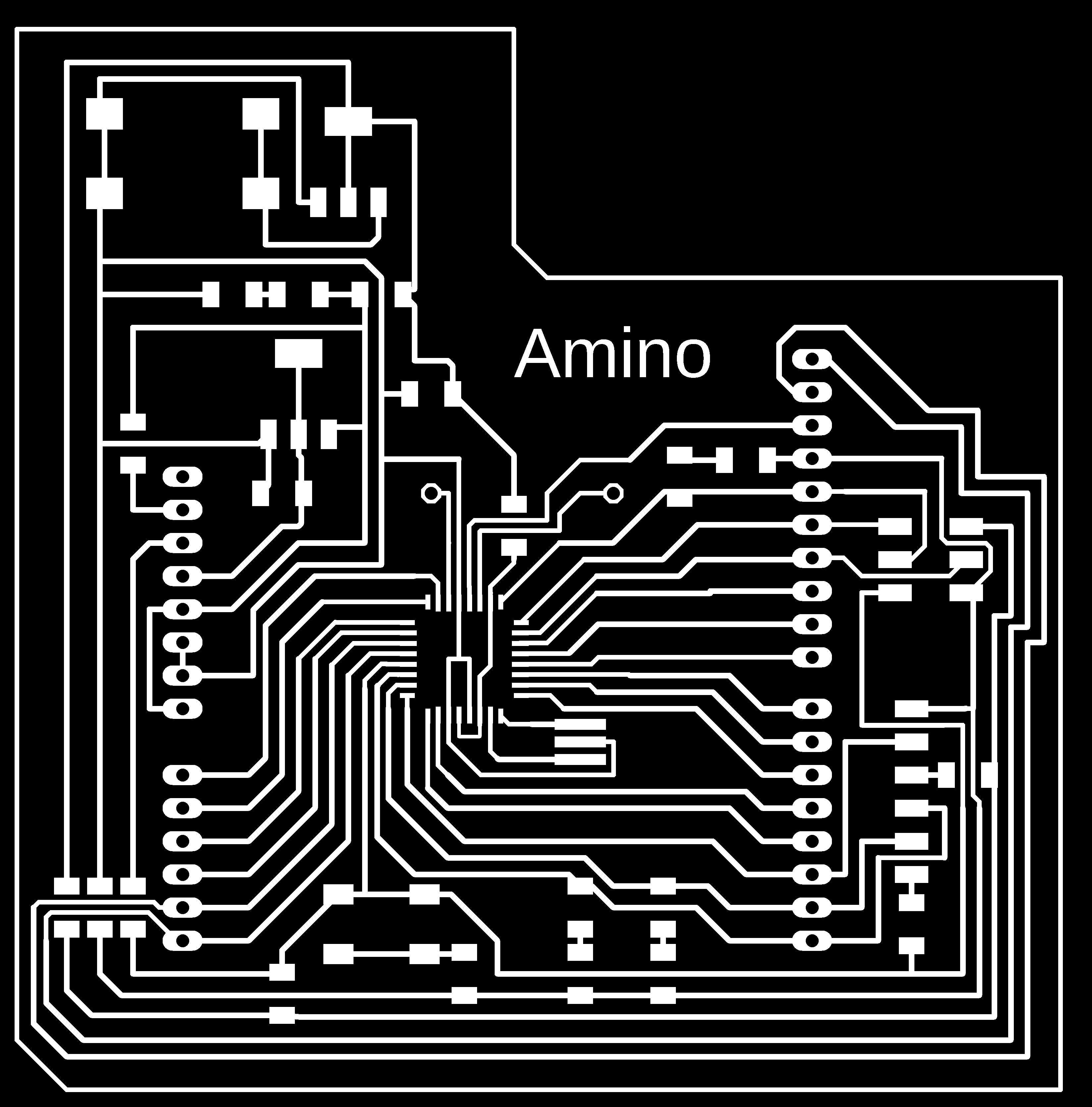
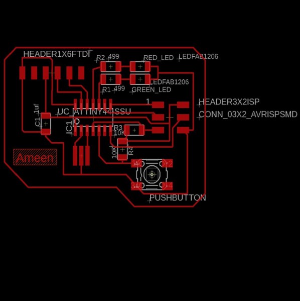
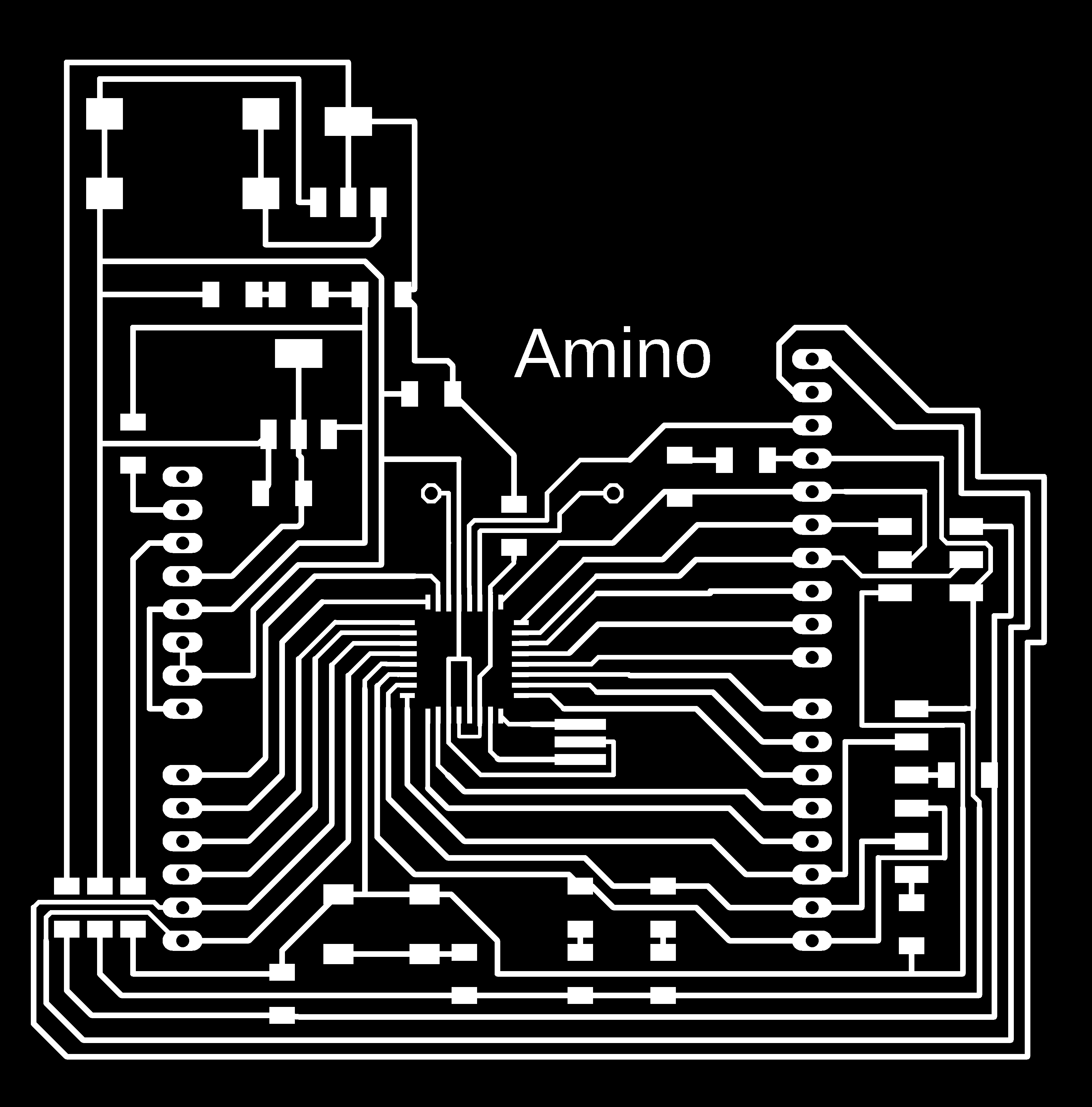
The figure below shows the schematic diagram of the board, which consists mainly of atmega 328 micro controllar, pin header and crystal 20 MHz. The table below the picture shows the components of the board.
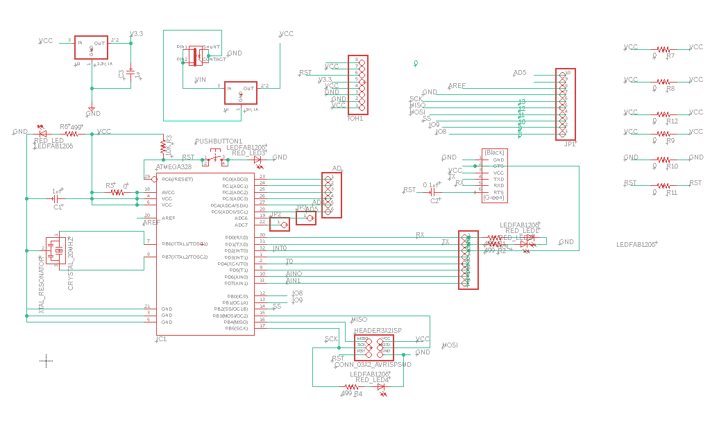
| Description | Reference | Lib Name | Quantity |
|---|---|---|---|
| ATMEGA328 | IC1 | TQFP32-08THIN | 1 |
| CRYSTAL_20MHZ | CRYSTAL_20MHZ | EFOBM | 1 |
| Header 3x2 ISP | HEADER3X2ISP | CONN_03X2_AVRISPSMD | 1 |
| Header 1x6 FTDI | U$1 | CONN_06_FTDI-SMD-HEADER | 1 |
| Capacitor unpolarized 1uF | C1 | CAP_UNPOLARIZEDFAB | 2 |
| Capacitor unpolarized 0.1uF | C2 | CAP_UNPOLARIZEDFAB | 2 |
| Resistor 499 Ohm | R1&R2&R4&R6 | R1206FAB | 1 |
| Resistor 0 Ohm | R5&R7&R8&R9 &R10&R11&R12 |
R1206FAB | 1 |
| Resistor 10kOhm | R3 | R1206FAB | 1 |
| RED_LED | RED_LED | LEDFAB1206 | 2 |
| blue_LED | blue_LED | LEDFAB1206 | 2 |
| yellow _LED | yellow_LED | LEDFAB1206 | 2 |
| JACK | J1 | PJ-002AH-SMT | 1 |
| Voltage regulator 3.3V | U2 | SOT223 | 1 |
| Voltage regulator 5V | U1 | SOT223 | 1 |
| PUSHBUTTON | PUSHBUTTON | 6MM_SWITCH | 1 |
| pin header 1X1 | JP2&JP3 | R1206FAB | 2 |
| pin header 1X6 | AD | R1206FAB | 1 |
| pin header 1X8 | TOH1 | R1206FAB | 2 |
| pin header 1X10 | JP1 | R1206FAB | 1 |
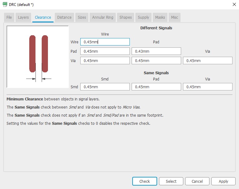
Before starting tracing, the design roles should be defined as below to avoid short circuit when milling the board. For more details Electronics design


Mods
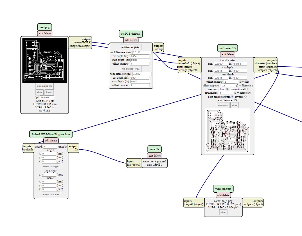
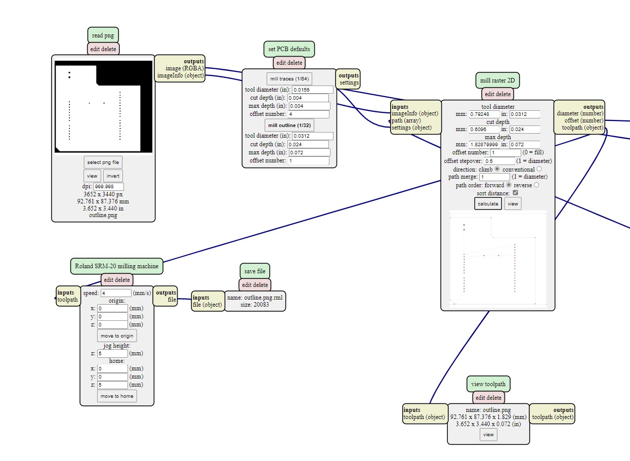
Step 1: Open Mod and Right click any whare. select programs - open server program - PCB png from Roland SRM-20 list.
Step 2: On the “read png” block Click on select png file and choose the "trace.png"
Step3: Select mill trace from “set PCB defaults” block.
Step4: On the “Roland SRM-20 milling machine” block let the origin coordinates 0,0,0
Step8: Right click and select modules - open server module- save.
Step9:- replace "websocte device" block with "save file" block .
Step10:- Click on calculate in "mill raster 2D" block , The RML file will be downloaded automatically.
Note : you can have better finish if you make the offset more than 4 like 6 but it will take more time.
Step11:Repeat the previous steps on the outline.png file, but click on the mill outline rather than mill traces from set PCB defaults block , to have outline.rml file
Note: check the job dimention before calculate.
VPanel for SRM-20 software (PCB)
Now we can mill and cut the board design using the rml files. first of all we must identify the mill bit's origin.
Step 1: Open the VPanel program and go to the dropdown menu and pick "Machine Coordinate System."
Step 2: move the head over the bottom left corner of the PCB, use the arrows in red box. then raise the head , use the "+Z" arrow to create enough space between the spindle and the PCB.
Step 3: Install the 1/64" milling bit in the spindle collet, keeping roughly 25% of its length outside.
Step 4: Using the "-Z" arrow, lower the spindle until the distance between the PCB and milling bit tip are about 5 mm . Untie the fastening screw while holding the milling bit between your fingers. Lower the milling bit until it makes contact with the PCB. Tighten the fastening screw.
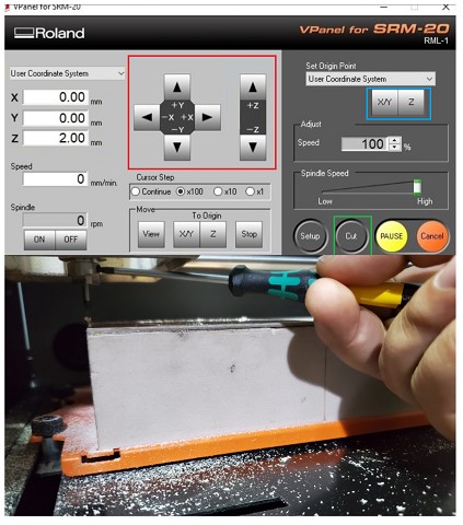
Step 5: Select "User Coordinate System" from the "Set Origin Point" by clicking on "XY" and "Z" in blue box . In the user coordinate system, this will make the current position the home or zero position.
Step 6: Move the milling bit a few millimeters above the PCB.
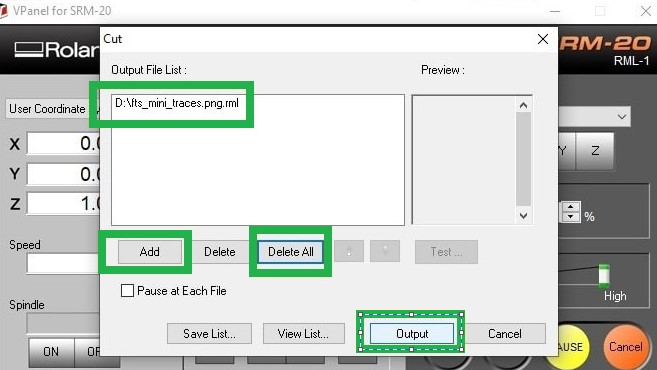
Step 7: Select "Cut" and then "Delete All" to get rid of any outdated jobs. Select the traces rml file by clicking "Add." finally Choose "Output" Now is the time for the machine to start.
Step 8: When the first job is finished, go to the "Move" menu and select "XY". The spindle will be moved to the "XY" home . lift up milling bit , cover it and remove it. after that install milling bit 1/32".
Step 9: Repeat steps 4 to 7 with "cut.png .rml" file, but don't change x , y coordinate for origin "home coordinate "
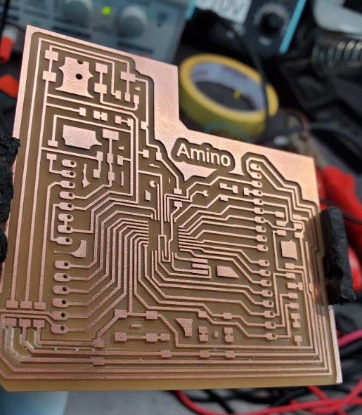
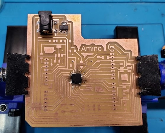
Rsults
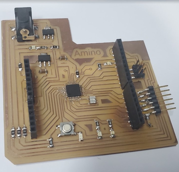
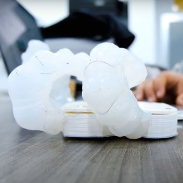
Soldering
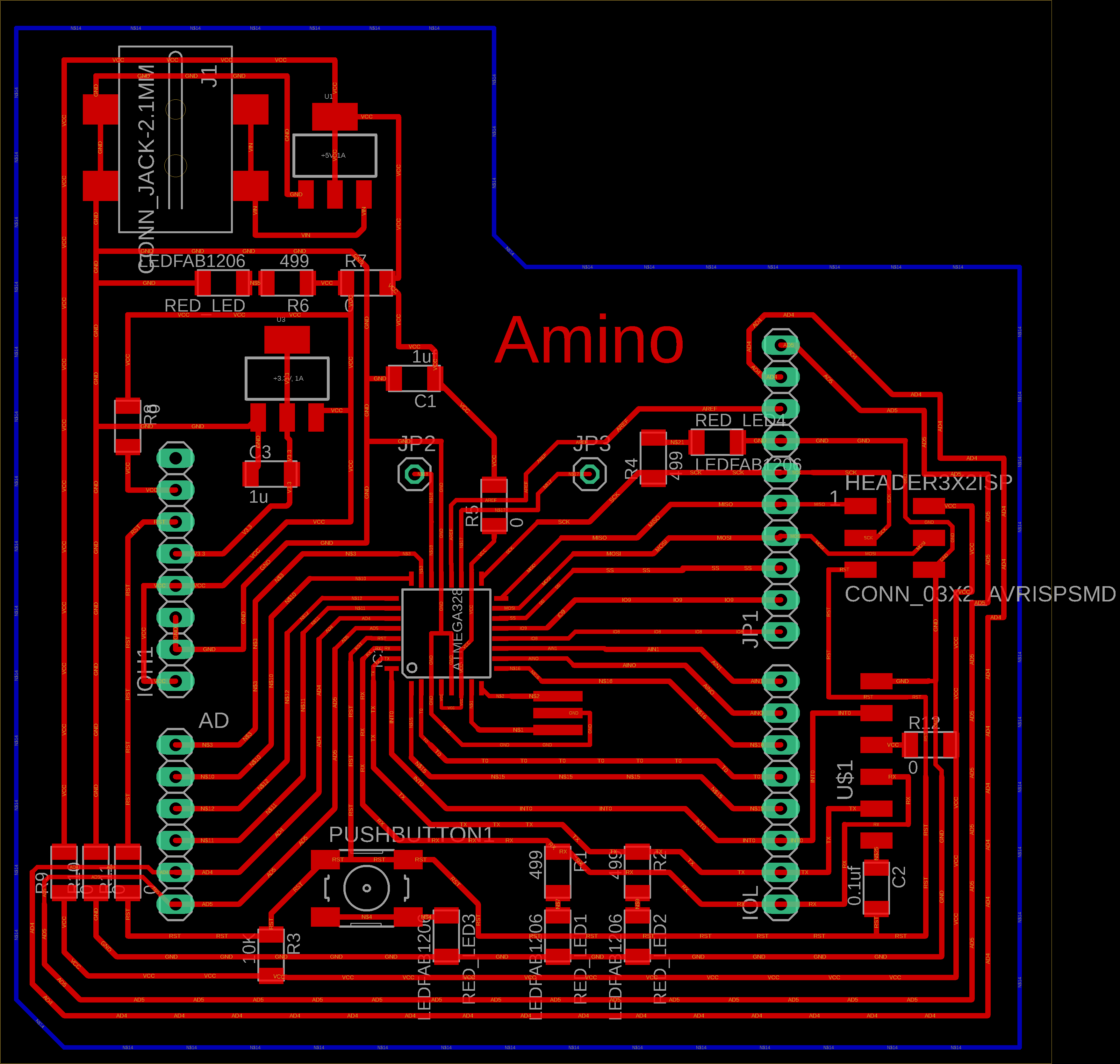
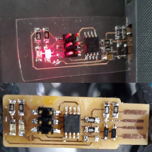
Use the schematic as a reference for component values and placement while soldering the parts to the PCB.
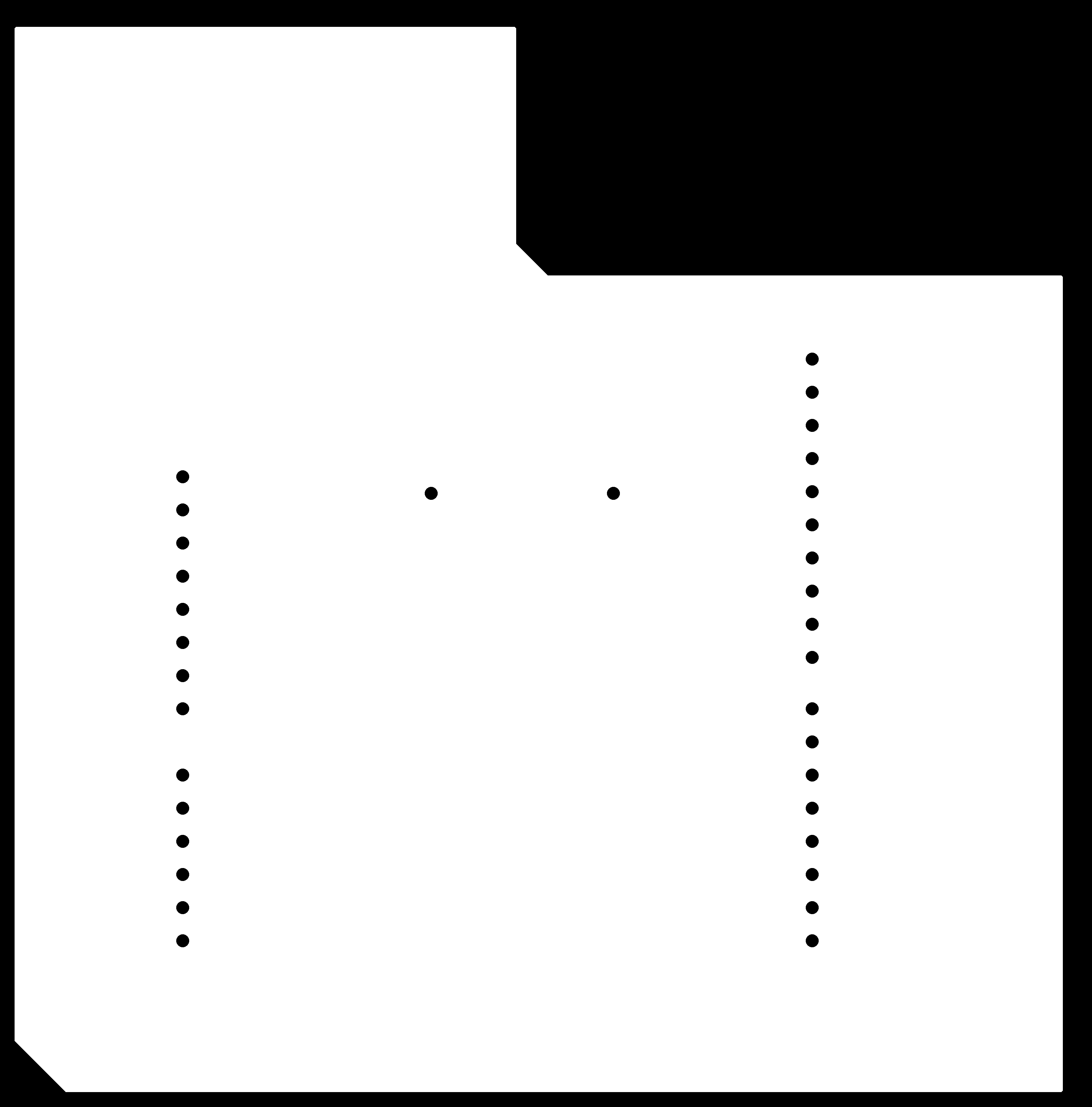
Note the components that must be installed in the correct orientation:
-The LED cathodes on the PCB drawing are marked with dots and thicker lines. If you do not find the dots and thicker lines , determine the cathode using a multimeter.
-The ATMEGA328 marks pin 1 with a dot laser-etched into the corner of the package. Pin 1 is marked in the drawing with a dot as well.


